PC Board Design for Low EMI in IoT Products
An increasing number of manufacturers are adding or retrofitting wireless technology into new or existing products. These products typically include mobile, household, industrial, scientific, and medical devices. This transition toward “everything wireless” is in full swing, and with it comes problems with EMI. That is, EMI from the product itself interfering with sensitive on-board cellular, GPS/GNSS, and Wi-Fi/Bluetooth receivers. This is called “platform” or self-interference, and it has become a big problem for manufacturers.
Wireless Self-Interference
Most of today’s digital-based products create a large amount of on-board RF harmonic “noise” (EMI). While this digital switching won’t usually bother the digital circuitry itself, that same harmonic energy from digital clocks, high-speed data buses, and especially on-board DC-DC switch-mode power supplies can easily create harmonic interference well into the 600 to 850 MHz cellular phone bands and even as high as 1575 MHz GPS/GNSS bands, causing receiver “desense” (reduced receiver sensitivity).
In order to use the various mobile phone services, manufacturers must pass very stringent receiver sensitivity and transmitter power compliance tests according to CTIA (Cellular Telephone Industries Association) standards. This on-board digital EMI and resulting receiver desense often delays product introductions for weeks or months.
Broadband and Narrow Band Interference
The two common types of high-frequency harmonic signals that can disrupt sensitive receivers are narrow band and broadband. Figure 1 shows the difference as we are looking from 1 to 1500 MHz. Typically, DC-DC converters or data/address bus noise will appear as a very broad-looking signal with several resonant peaks (violet trace), while crystal oscillators or high-speed clocks will appear as a series of narrow spikes (aqua trace). The broadband sources can be more easily observed when placing the spectrum analyzer in “Max Hold” mode. Unless the product is designed for EMI compliance, both these types of signals can radiate or conduct high-frequency energy well into the mobile phone, GPS, or other wireless bands. (See Reference 1 for more information on characterizing self-generated EMI at the board level.)
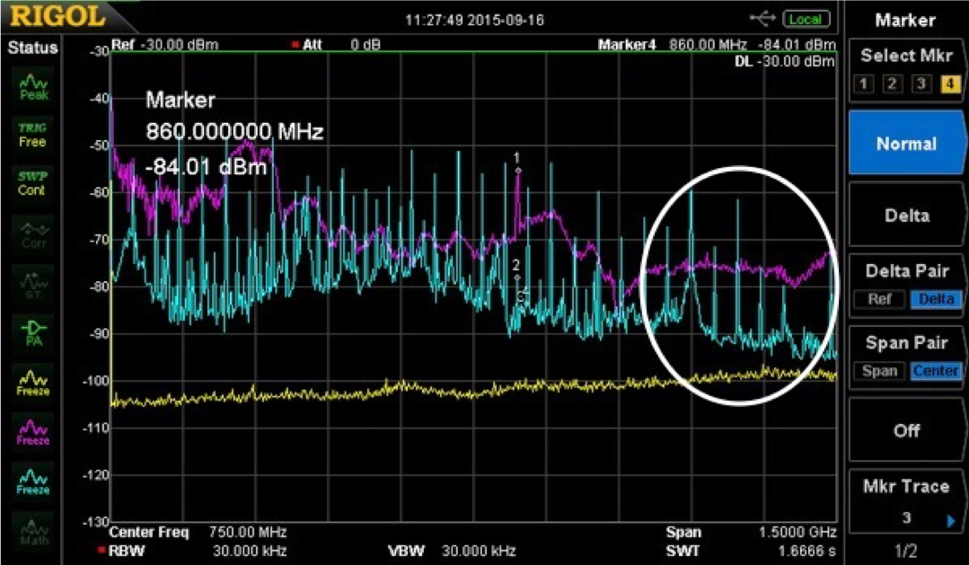
Fig. 1 There are two common types of high-frequency harmonics; broadband (violet trace) and narrow band (aqua trace). In this example, we are looking from 1 to 1500 MHz to generally characterize the spectral emissions profile of a DC-DC converter (violet trace) and an Ethernet clock signal (aqua trace). The ambient noise floor is indicated by the yellow trace at the bottom. Both sources of EMI will potentially cause interference to the U.S. 600 to 850 MHz cellular and GPS bands (indicated by the area enclosed by the white circle.) The Ethernet harmonics have peaks that are more than 40 dB over the ambient noise level within the cellular band.
Sources of Platform (or Self-Generated) EMI
There are generally two primary areas of focus where on-board energy sources can couple to the receiver antenna or wireless module and cause loss of receiver sensitivity (see Figure 2):

Fig. 2 A typical IoT product showing the two major coupling paths, radiated and conducted.
1. On-board energy sources, such as DC-DC converters, address and data buses, and other fast-edged digital signals that can conduct or couple this EMI directly to wireless modules or their antennas.
2. Attached I/O or power cables that act as “radiating structures” (antennas) that couple this self-generated RF energy directly into on-board or attached wireless antennas.
Very often, the electromagnetic (EM) fields are coupled directly within the board due to poor stack-up, poor functional circuit partitioning (RF, digital, power conversion), or poor signal/power routing. It is also very possible that stray electromagnetic fields are simply coupling directly into the antenna. It could also be a combination of both.
Designing PC Boards for Low EMI
If you’re developing IoT products, poor PC board design can cause endless delays due to on-board energy sources disrupting sensitive receiver circuits resulting in cellular compliance failures. GPS and Wi-Fi receivers can also lose sensitivity.
There are many factors that contribute to poor EMI designs on PC boards. These include:
1. Mixing noisy circuits, such as power and motor conversion with digital and sensitive analog circuits
2. Locating clock drivers too close to board edges or near sensitive circuits
3. Poor trace routing which leads to crosstalk
4. Running clock (or high-speed) traces over gaps/slots in the return plane
5. And above all, incorrect layer stack-ups
I have already addressed crossing clock traces over gaps in the return plane (References 2 and 3). However, fixing this last item regarding layer stack-ups will usually correct a myriad of ills, including many of the other items on the list.
Most of us electrical engineers were taught incorrectly how DC and AC current works in lumped or distributed (transmission line) circuits. Before we understand how signals propagate in PC boards, we must first understand some physics.
We were likely all taught (or at least it was implied) that “current” was the flow of electrons in copper. While this is correct for pure DC circuits, once we start considering AC (at least higher than 10 to 50 kHz) the signal energy is actually propagated as electromagnetic waves in the dielectric space between the copper traces and return plane. We now need to think of the copper traces as “waveguides” rather than circuits carrying electron current. This makes it vital to design an unbroken return path for the EM wave, otherwise, we’ll get field leakage (crosstalk or coupling) between various circuit functions.
The Physics of Signal Propagation
First, consider how capacitors seemingly allow the flow of electrons. After all, isn’t that how decoupling capacitors work? Referring to Figure 3, if we apply a battery to the capacitor, any positive charges applied to the top plate will repel positive charges on the bottom plate, leaving negative charges. If we were to apply an AC source to the capacitor, it would seem that current is flowing through the dielectric—a seeming impossibility. James Maxwell called this “displacement current,” where positive charges merely displace positive charges on the opposite plate leaving negative charges, and vice versa. This displacement current is defined as dE/dt (changing E-field with time).
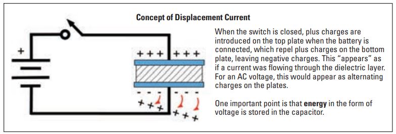
Fig. 3 The concept of displacement current through a capacitor.
The next thing to realize is that electrons do not travel near light speed in copper as we were taught, but move at about 1 cm/sec, due to the very tight atomic bond of the copper molecules (References 4 and 5). There are certainly clouds of free electrons, but these move slowly from molecule to molecule. This is called conduction current and is what we would measure with an ammeter. Conduction current is related to the tangential component of the B-field, that is the curl B = J.
However, the influence of one electron in the copper molecule to its neighbor (and on down the transmission line) propagates at the speed of the EM field in the dielectric material. In other words, jiggle one electron at one end of a microstrip, and it jiggles the next, which jiggles the next, and so on, until it jiggles the last one at the end. This jiggling is called a kink in the E-field and can be envisioned as the Newton’s Cradle toy, a mechanical analogy, where the first ball is raised and released, then hits the next ball, etc., and this eventually pops off the end ball.
How Digital Signals Propagate
Consider a digital signal with a wave front moving at about half light speed (about a typical 6 in./ns in FR4 dielectric) along a simple microstrip over an adjacent return plane as illustrated in Figure 4.
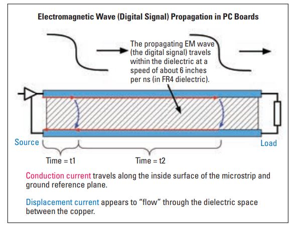
Fig. 4 The digital signal (an electromagnetic wave) travels through the dielectric space between the microstrip and return plane at about half light speed (~6 in./ns) in FR-4 dielectric.
The next realization is that the EM field of the digital signal travels in the dielectric space—not the copper! The copper merely “guides” the EM wave (References 5 and 6).
When the signal (EM wave) is first applied between the microstrip and return plane, it starts to propagate along the transmission line. There is a combination of conduction current and displacement current (across the dielectric).
All the exciting “EMI stuff” happens at the wave front as the EM wave propagates. At any instant in time, the electric field behind the initial wave front is stable at whatever the applied voltage is at the moment, and the electric field in front of the initial wave front is zero. The fast rise or fall times of the signal contain all the harmonic energy, and this is what generates the EMI.
If the load impedance is equal to the characteristic impedance of the transmission line, then there will be no reflections of the EM wave back to the source. However, if there is a mismatch, there will be reflected EM fields propagating back to the source. In reality, most digital signals will have multiple reflections moving back and forth through the transmission line simultaneously. The transition zone (rise time or fall time) of these propagating waves will produce EMI (Reference 5).
Rules For Transmission Lines
Now realizing how digital signals move in circuit boards, there are two very important principles when it comes to PC board design:
1. Every signal and power trace (or plane) on a PC board should be considered a transmission line.
2. Digital signal propagation in transmission lines is really the movement of electromagnetic fields in the space between the copper trace and the return plane.
In order to construct a transmission line, we must have two adjacent pieces of metal in order to capture or contain the field. For example, this could be a microstrip over an adjacent return plane, a stripline adjacent to a return plane, or a power trace (or plane) adjacent to a return plane. Locating multiple signal layers between power and return planes will lead to real EMI issues for fast signals, as well as coupling power bus transients to the signals. Observing these two rules will dictate the layer stack-up!
In other words, every signal or power trace (routed power) must have an adjacent return plane and all power planes should have an adjacent return plane. Multiple return planes should be tied together with an array of stitching vias (Reference 7).
A discontinuity, such as a gap or slot, in the return path for conduction current may cause some of the signal field energy to leak into the dielectric space, leading to edge radiation from the board and cross-coupling to other circuits through via-to-via coupling. This also occurs when we pass a signal through multiple ground reference or power planes if there is no adjacent stitching via or stitching capacitor (to connect return planes to power planes).
Stack-Up Design for Low EMI
The stack-up design is key to designing a low EMI board.
Typical Four-Layer Design: One four-layer stack-up frequently seen is shown in Figure 5. This probably worked fine in the 1990s through early 2000s, but with today’s much faster and mixed-signal technologies, with clock frequencies over 50 MHz, it may be a recipe for EMI disaster. There are two issues with this: the bottom signal layer is referenced to the power plane and the power and ground return planes are too far apart.

Fig. 5 This very common, but poor, four-layer board stack-up is a recipe for EMI disaster!
With few exceptions (some DDR RAM use Vtt as the return plane, for example) signals use ground as their return path. Using the power plane as the return path is very EMI-risky, because return currents may have to flow between the power and ground planes when the signal traces change layers. These currents would have to flow through the decoupling capacitors which have low impedance only below about 50 MHz at best.
The following are two ideas for PC board stack-ups that maintain good return path control.
One good four-layer board stack-up for improved EMI is shown in Figure 6. Instead of a power plane, we use either routed or poured power, along with signals on layers 2 and 3. Thus, each signal/power trace is adjacent to a return plane. Also, it is easy to route signals between the two layers, so long as the two return planes are connected together with an array of stitching vias. If you run a row of stitching vias along the perimeter (say, every 5 mm) you will form a Faraday cage. One caution is that the top ground return plane (component side) will often require many holes in order to clear component leads. Make sure these holes include copper between them to avoid creating long gaps.

Fig. 6 A good four-layer board stack-up for improved EMI, with return planes on outer layers.
If, on the other hand, you’d prefer to have access to the signal and routed/poured power traces, you may simply reverse the layer pairs, such that the two return plane layers are in the middle and the two signal layers are positioned at the top and bottom, with routed power and sufficient decoupling caps, rather than a power plane (see Figure 7).
Fig. 7 A good four-layer board stack-up for improved EMI, with return planes on inner layers.
For both four-layer designs, you want to run an array of stitching vias connecting the two return planes about 5 to 10 mm apart, maximum. This is a quarter wavelength spacing for frequency components in the 10 GHz range.
Typical Six-Layer Design: Another stack-up I frequently see is this six-layer design (see Figure 8). Again, there are two issues with this: the bottom two signal layers are referenced to the power plane and the power and ground return planes are non-adjacent and too far apart.
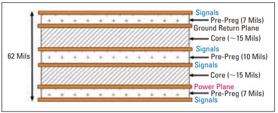
Fig. 8 A very common, but poor EMI, six-layer stack-up design. Signal layers 4 and 6 are referenced to power, while the return and power planes are non-adjacent with two signal layers in between. This will couple power transients on those two signal layers.
Once again, we have signals referenced to power, so there is a return path discontinuity when signals change return planes. As in the four-layer design (Figure 5), the power and return planes are too far apart and are now separated by two signal layers. Any power network transients will cross-couple within the dielectric layers, coupling to any signal traces on layers 3 and 4 along the way.
Both the suggested four- and six-layer board designs above (Figures 6, 7, and 9), follow the two fundamental rules, which preserve good return path design. All multiple return planes should be stitched together with a 5 to 10 mm array of vias.
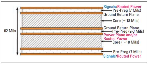
Fig. 9 An improved six-layer board stack-up design. There are other iterations that will work, so long as the two basic design rules are met.
Of course, there are many more iterations on creating proper transmission line pairs between signal and return plane or power and return plane. Rick Hartley offers an excellent two-day seminar on PC board and stack-up design (Reference 8).
What About Two-Layer Boards? Simple, just run signals and routed power on layer 1 and use a return plane on layer 2. When signals need to cross under a trace, short “cross-under” paths can be routed in the bottom ground plane. This is really one and a half layers of routing.
Partitioning and Routing
This section addresses partitioning of circuit sections, routing of high-speed traces, and a few other layout practices to help reduce EMI. Besides proper layer stack-up, the next most important consideration when laying out the circuitry on your board is partitioning circuit functions, such as digital, analog, power conversion, RF, motor control, or other high-power circuits.
First, we must understand and visualize how return currents flow and how the EM fields are distributed with high-speed circuit traces. At frequencies below about 50 kHz, return currents tend to follow the path of lowest resistance. Thus, they tend to travel along the shortest resistive distance between source and load, as simulated by the green area in Figure 10.

Fig. 10 A meandering surface trace over a plane with contacts to the return conductor at either end. The colors represent the return current distribution simulated at 1 kHz. Image, courtesy Keysight Technologies.
At frequencies above 50 to 100 kHz, return currents tend to follow the path of lowest impedance due to mutual coupling effects between the signal and return paths. Thus, they tend to travel directly underneath the signal path between source and load, as simulated by the green area in Figure 11.
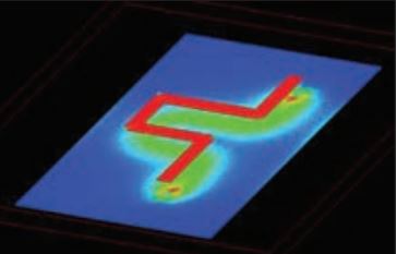
Fig. 11 Return current field distribution simulated at 1 MHz. Image, courtesy Keysight Technologies.
You can now understand why analog circuitry should be located well away from digital or other noisy circuits. We must keep these “spread out” return currents from intermixing with the return currents from noisy circuitry. That is why partitioning is so important.
To avoid EM field (signal) coupling and crosstalk, we must avoid allowing fields to intermix within the same dielectric space. Figure 12 demonstrates one example of partitioning major circuit functions. Of course, this gets more challenging as the board size is reduced. Henry Ott also describes this concept in Reference 10.

Fig. 12 One example of practical partitioning of circuit functions for an IoT product.
Partitioning is especially important when it comes to mixed-signal designs, such as a combination of analog and digital or wireless and digital. Many of my clients combine wireless along with digital processing and sometimes analog (audio amplifiers or video, for example). For small mobile or IoT devices, the importance of adequately partitioning circuit functions becomes mandatory to eliminate digital switching currents from interfering with sensitive receivers.
Knowing that low-frequency signal returns tend to spread out more, we can see that any analog or low-frequency circuitry must be separated from digital, power conversion, or motor controller circuits. Likewise, sensitive RF receiver circuits, such as GPS, cellular, or Wi-Fi devices must also be kept separate from digital, power conversion, or motor controller circuitry, as well.
The concept of partitioning is easy to understand, but actually implementing it can be tricky. An example is routing clocks. We probably do not want to run Ethernet and USB clocks all across our board. So, one important aspect would be to locate these I/O functions closest to their associated connectors, as in Figure 12.
Usually, we like to locate switch-mode power supply (SMPS) away from sensitive RF or analog circuitry. However, in some cases, it may make more sense to locate SMPS circuitry closer to what they power. It is vital, though, to ensure all SMPS circuitry runs on the same layer with an adjacent return plane. (Recommendation: avoid locating SMPS circuitry too close to wireless modules or circuits, especially antennas.)
In Figure 12, power distribution is indicated by blue lines. Actually, the power distribution on real boards will likely be a combination of power planes (3.3 V is typical) and power polygons or routed wider traces for the other required power rails. This power distribution should also have an adjacent return plane in order to contain any transient fields due to “ground bounce” switching currents.
Separating RF from Digital in Small IoT Products
Because of skin effect, where high-frequency currents tend to flow along just the surface of a trace or plane, it is possible to use both sides of a return plane to isolate signal or power-return currents. Theoretically, you could run “noisy” signals on adjacent traces above a plane and “quiet” signals on adjacent traces below that same plane, and the two should not couple.
Here is one stack-up idea that uses this concept and has been used successfully by mobile device manufacturers (see Figure 13). If we populate the top side of the board with all the RF/wireless components and the bottom side with the digital, power conversion, and control (while being careful to add return paths to all signals transitioning from top to bottom), field energy from the top should not contaminate the bottom and vice versa.
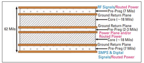
Fig. 13 The concept of partitioning by separating noisy digital circuits on the bottom side from contaminating sensitive RF circuits on the top side.
Note that we keep the main power distribution (usually 3.3 V) in the center of the stack-up. Very complex circuitry or larger layer stack-ups will likely require additional power/return plane layers, which are best located near the top and bottom layers, depending on the number of circuit functions. One recent example I helped with was a mobile video platform with cellular, Wi-Fi, Bluetooth, digital video and audio, and it used a 10-layer stack-up in order to separate functional blocks. Of course, there are many ways to accomplish this objective. Figure 13 is only one example.
Routing Techniques and Other Issues
Gaps in Return Planes: All return planes should be as solid as possible and designed without long gaps or slots (see Figure 14). When a high-frequency trace crosses a gap in the return path, it creates a source of common mode currents, which generally couple all over the board and create the potential for radiated emissions failures and coupling to sensitive receiver modules. See References 2 and 3.

Fig. 14 There are two issues in this example; we have a digital signal crossing two gaps in the ground plane (GRP) and it also crosses a “quiet” analog plane.
The gap also causes field leakage within the dielectric space, which can couple to nearby vias from other signals, causing unwanted coupling. It also causes “edge radiation” directly from the board into antennas. The efficiency of the radiated emissions increases as the harmonic frequency of the common mode currents approaches 1/4 to 1/2 wavelength of either the cables or board dimension. See Reference 11.
Splitting Planes: Many A/D and D/A manufacturers suggest splitting analog and digital planes as a way to isolate digital noise currents from sensitive analog signals (see Figure 15).
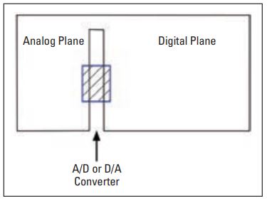
Fig. 15 A split-plane concept is often suggested for A/D or D/A circuits.
This is still an ongoing debate, and my opinion is that there are certain conditions that would warrant this technique, such as low-level audio circuitry in automobile infotainment systems, where you would want the analog return isolated from the digital return. But for most designs, if you use partitioning correctly, it will inherently provide isolation between noisy and sensitive circuit functions, even for A/D and D/A applications. For these latter cases, it is important to keep the analog traces away from the digital traces. Obviously, we do not want to run traces of any kind across the gap.
The real issue when separating planes is that there may be some high-frequency voltage differential between the two. If the planes with their connecting I/O cables approach a significant fraction of a half-wavelength, it can be modeled as a dipole antenna and lead to radiated emissions and various immunity issues (see Figure 16).

Fig. 16 Two separate planes may have an RF voltage potential between them and then radiate like a dipole antenna.
One of the few exceptions (and there are a few others, such as remote sensors) is the need for patient isolation for line-operated medical equipment. Figure 17 shows a typical ground return diagram where the analog probe processing is referenced to analog return, the digital processing circuitry is referenced to digital return, and the power supply is referenced to Earth. The digital and power returns would ideally be connected together at the power connector. The isolation device could be a specialized isolated coupler IC, an optical coupler, or several other similar devices.

Fig. 17 A typical grounding configuration for a patient-connected monitor.
Other Guidelines to Minimize EMI
Clock Oscillators/Crystals/Drivers: These should be located toward the center of the board (or digital partition), as close to the device they are driving, and away from board edges and especially I/O or power connectors.
Clock Traces: all clock traces should be short and direct. Avoid running these along board edges because that can physically couple to the board edge and cause board resonances and consequent board radiation.
I/O and Power Connectors: I/O and power connectors should be located along a single edge of the board and located as close to one another as possible. As connectors are spaced further apart, the chances of increasing EMI-related RF voltage can be measured from one connector body to the other. With cables attached, this can be modeled as an RF source driving a dipole antenna. We want to minimize the RF voltage drop between all connectors by locating them close together. The worst case would be to have connectors located on each side of a board with noisy sources driving common currents to the attached cables.
RF Module Transmission Lines: All antenna transmission lines should be run short and direct to the antennas or antenna port connectors. These may be buried in between two return planes and may dictate eight, or more, layers in order to achieve a 50-Ohm impedance through “keep out” areas in the layers immediately above and below the transmission line(s). Usually, it is best to follow the module manufacturer’s guidance.
Ethernet Connectors: Usually, there should be a void in the ground return (and power) plane directly underneath Ethernet connector magnetics in order to reduce noise capacitive coupling from the board. However, there may be special cases where the connector manufacturer suggests otherwise, especially, if common current-diverting capacitors are included to the return plane under the connector for additional EMI suppression. In that case, the return plane should be extended only up to the capacitors.
Urban Legends
Multiple Decade-Spaced Decoupling Capacitors: Adding a series of (usually) three capacitors, such as, 10, 1, and 0.1 μF capacitors (or similar) on power pins of ICs was thought to help even out the frequency response and lower the overall impedance in the power distribution network. All that actually does is create the potential for parallel resonances due to the various series interconnect inductances (Reference 12). It is best to stick with equal values.
Ground Pours (or Fill): Despite many who recommend this, it is not always a good practice to fill all spaces between signal traces with “ground pours.” It seldom actually helps and there is a chance it could result in higher cross talk due to resonant coupling between traces. (Reference 18).
90-Degree Turns: It has been pretty well proven that for normal digital traces (at least to a few GHz), it is not necessary to chamfer or round off corners. It is all right to make 90-degree bends where needed (References 13, 14, and 15).
20H Rule: There is also the so-called “20H Rule,” where the power plane should be set back from the edge of the return plane by 20 times the dielectric thickness (h). This supposedly helped reduce fringing fields. If nothing else, aligning the planes allows the possibility of adding shorting vias between all the ground planes. (References 16 and 17).
Summary
In practice, designing real PC boards for complex circuits requires some understanding of EM fields. There will always be trade-offs between partitioning of circuits, stack-up decisions, and routing of power and high-frequency signals. However, if the basic design rules are followed:
1. Keep an adjacent return plane for both signal and power distribution layers.
2. Engineer a low impedance return path when transitioning signals through layers.
3. Partition different circuit functions as best you can.
Then you will have a greater chance of keeping noisy signals away from quiet ones, and the risk of radiated emissions, radiated immunity, ESD, and wireless self-interference is greatly reduced.
Most of the projects I’ve been fortunate enough to work on recently have been IoT products, where partitioning and getting the circuit board stack-up and routing designed correctly from the start is so very important for success, not only for reduced EMI, but for proper receiver sensitivity of on-board wireless and IoT receivers.
Remember, high-frequency digital signals travel within the dielectric space, not through the copper. This will dictate the stack-up design. Once you realize this, you can avoid the issue of noisy digital signals sharing the same dielectric space as low-level analog or RF signals and there will be a much greater chance of getting it right the first time.
I’d like to acknowledge the assistance and learnings from physicist, Ralph Morrison (Reference 19), who realized years ago that fields must be considered when designing circuit boards and Rick Hartley, who teaches an excellent two-day seminar on PC board design for low EMI and best signal integrity. I also appreciate the help of Daniel Beeker, senior applications engineer at NXP Semiconductor and Dr. Eric Bogatin, Signal Integrity Journal’s technical editor as well as signal integrity evangelist at Teledyne LeCroy and adjunct professor at the University of Colorado, Boulder, who both helped beat this concept of field theory into my head.
References
1. K. Wyatt, “Characterizing & Debugging EMI Issues for Wireless and IoT Products,” Signal Integrity Journal, July, 2019, https://www.signalintegrityjournal.com/articles/1335-characterizing-debugging-emi-issues-for-wireless-and-iot-products.
2. P. André and K. Wyatt, “EMI Troubleshooting Cookbook for Product Designers,” Scitech Publishing, 2014.
3. K. Wyatt and R. Jost, “Electromagnetic Compatibility EMC Pocket Guide,” Scitech Publishing, 2013.
4. R. Schmitt, “Electromagnetics Explained – A Handbook for Wireless/RF, EMC, and High Speed Electronics,” Newnes, 2002.
5. E. Bogatin, “Signal Integrity – Simplified (3rd edition),” Prentice Hall, 2018.
6. R. Morrison, “Digital Circuit Boards – Mach 1 GHz,” Wiley, 2012.
7. R. Morrison, “Fast Circuit Boards – Energy Management,” Wiley, 2018.
8. R. Hartley, Control of Noise, EMI and Signal Integrity in PC Boards (two-day seminar), Rick Hartley Enterprises, managed by https://www.pcb2day.com.
9. D. Beeker, “Effective PCB Design: Techniques To Improve Performance,” https://www.nxp.com/files-static/training_pdf/WBNR_PCBDESIGN.pdf.
10. H. Ott, “Electromagnetic Compatibility Engineering,” Wiley, 2009.
11. K. Wyatt, “Gaps in Return Planes,” https://www.youtube.com/watch?v=L44lTnQgv-o&t=9s.
12. E. Bogatin, L. Smith, & S. Sandler, “The Myth of Three Capacitor Values,” Signal Integrity Journal, March, 2020, https://www.signalintegrityjournal.com/articles/1589-the-myth-of-three-capacitor-values.
13. H. Johnson, “Who’s Afraid of the Big Bad Bend?”, SigCon, http://www.sigcon.com/Pubs/edn/bigbadbend.htm.
14. Altium, “PCB Routing Angle Myths: 45-Degree Angle versus 90-Degree Angle,” 2018, https://resources.altium.com/pcb-design-blog/pcb-routing-angle-myths-45-degree-angle-versus-90-degree-angle.
15. E. Bogatin, “When to Worry About Trace Corners: Rule of Thumb #24,” EDN, February, 2015, https://www.edn.com/electronics-blogs/all-aboard-/4438573/When-to-worry-about-trace-corners--Rule-of-Thumb--24.
16. H. Chen, et al, “Effects of 20-H Rule and Shielding Vias on Electromagnetic Radiation from Printed Circuit Boards,” archived at SpeedingEdge, https://speedingedge.com/PDF-Files/epep_20hrule.pdf.
17. H. Shim and T. Hubing, “20-H Rule Modeling and Measurements,” Missouri University of Science & Technology (archived at Clemson University), https://cecas.clemson.edu/cvel/pdf/EMCS01-939.pdf.
18. E. Bogatin, “Seven Habits of Successful 2-Layer Board Designers,” Signal Integrity Journal, April, 2019, https://www.signalintegrityjournal.com/blogs/12-fundamentals/post/1207-seven-habits-of-successful-2-layer-board-designers.
19. R. Morrison, https://www.ralphmorrison.com.
Published in the SIJ July 2020 Print Issue, Special Report: Page 24.